
More Information
Submitted: June 19, 2025 | Approved: June 30, 2025 | Published: July 01, 2025
How to cite this article: Alaskari MKG, Sepehri A, Kassaee MZ. Topological and Topographical Orders in Twisted Graphene: Pathways to Quantum and Electronic Innovations. Int J Phys Res Appl. 2025; 8(7): 211-220. Available from:
https://dx.doi.org/10.29328/journal.ijpra.1001128
DOI: 10.29328/journal.ijpra.1001128
Copyright license: © 2025 Alaskari MKG, et al. This is an open access article distributed under the Creative Commons Attribution License, which permits unrestricted use, distribution, and reproduction in any medium, provided the original work is propeRLy cited.
Keywords: Twisted bilayer grapheme; Topological order; Topographical order; Quantum properties; Electronic applications; Structural characterization

Topological and Topographical Orders in Twisted Graphene: Pathways to Quantum and Electronic Innovations
Mohammad Kamal Ghassem Alaskari1*, Amir Sepehri2 and Mohammad Zaman Kassaee3
1Department of Petroleum Engineering, Petroleum University of Technology, Tehran, Iran
2Department of Petroleum Engineering, Islamic Azad University Science and Research branch, Tehran, Iran
3Department of Chemistry, Tarbiat Modares University, Tehran, Iran
*Address for Correspondence: Mohammad Kamal Ghassem Alaskari, Department of Petroleum Engineering, Petroleum University of Technology, Tehran, Iran, Email: [email protected]
Graphene has recently attracted considerable attention across fundamental science and engineering disciplines due to its exceptional properties, including superior electrical conductivity, thermal stability, optical transparency, and mechanical strength. These characteristics have positioned graphene as a key material in the advancement of next-generation electronic technologies.
In this paper, we present a comprehensive overview of graphene’s electronic and thermal properties, emphasizing its high conductivity, the quantum Hall effect, Dirac fermions behavior, high thermo power, and phenomena associated with magic-angle Twisted Bilayer Graphene (TBG). We also highlight emerging applications of twisted bilayer graphene in optical devices, electronic components, and thermal sensors. These developments hold great promise for future advancements in biomedical engineering, targeted therapies, environmental monitoring, and even fundamental physics.
A particularly compelling aspect of graphene is its topological order, which arises from its unique band structure. Unlike conventional conductors that facilitate free electron flow throughout the bulk, topologically ordered graphene supports robust edge states—conductive channels at the boundaries of two-dimensional systems that remain stable despite impurities or defects in the bulk material. This resilience is rooted in the material’s topological band structure and reflects principles from topology, the mathematical study of spatial properties preserved under continuous deformation.
Topological order in graphene exhibits remarkable resistance to environmental perturbations, making it a strong candidate for quantum electronic devices and quantum computing applications, particularly in preserving qubit coherence. Additionally, topographical order, including surface roughness and morphological features, plays a role in stabilizing edge states and influencing electronic behavior. Together, the topological and topographical orders enhance graphene’s potential for long-term quantum information retention.
This study explores the synthesis and characterization of twisted graphene structures, demonstrating significant enhancements in electronic performance. Structural and compositional properties were investigated using advanced techniques such as X-ray Diffraction (XRD), UV-Visible spectroscopy, Raman spectroscopy, Field-emission Scanning Electron Microscopy (FE-SEM), Transmission Electron Microscopy (TEM), and Atomic Force Microscopy (AFM). The results confirm that graphene’s unique electrochemical and mechanical features contribute to its robust electronic states.
In physics, order refers to the presence of organized or correlated structures within a system. Broadly speaking, physical order can arise from either space-time symmetries-such as those found in super symmetric or transformation-invariant systems-or from correlated states, which may exhibit long-range or short-range correlations depending on how order parameters decay with distance.
In condensed matter physics, ordered phases typically emerge at low temperatures. Upon heating, these systems may undergo one or more phase transitions into less ordered or disordered states. Common examples of such phase transitions include:
- Melting of ice: a transition from solid to liquid, involving the breakdown of translational order.
- Demagnetization of iron above the Curie temperature: a transition from ferromagnetic to paramagnetic states, representing a change in magnetic order.
These transitions may affect different types of physical order, such as:
- Translational order (e.g., crystalline lattice formation),
- Rotational or polar order (e.g., Ferro electricity),
- Spin order (e.g., magnetism), and other forms depending on the system under consideration.
1.1 Edge states and band gaps
Edge states are topologically protected electronic states that occur at the boundaries of certain low-dimensional materials (Figure 1). These states are robust against local perturbations and cannot be removed without violating the system’s underlying symmetry [1,2].
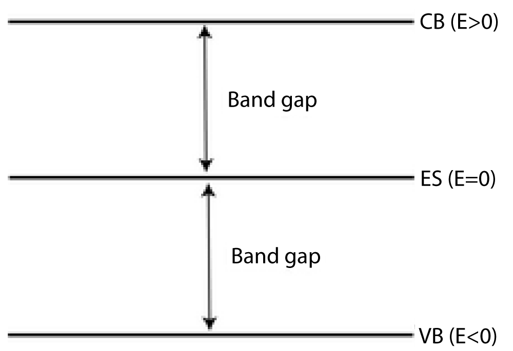
Figure 1: Schematic illustration of edge states in a typical two-dimensional material. The Conduction Band (CB), Edge States (ES), and Valence Band (VB) are associated with positive, zero, and negative energy net values, respectively.
The electronic band structure of a material is typically characterized by the band gap—the energy difference between the highest occupied states in the valence band and the lowest unoccupied states in the conduction band. This structure is obtained by solving the system’s Hamiltonian, which yields discrete energy levels (net values) and their associated wave vectors (net vectors).
- Conduction band: Energy levels where E > 0 (high-energy, delocalized states)
- Valence band: Energy levels where E < 0 (low-energy, typically bound states)
- Edge states: In certain materials, such as monolayer graphene or zigzag-edged graphene quantum dots, there exist states with E = 0. These zero-energy edge states lie within the band gap and significantly influence the material’s electronic, optical, and magnetic properties [3-5].
The presence of edge states leads to enhanced electrical conductivity along boundaries and may also contribute to exotic quantum effects, making them of great interest for applications in topological insulators, quantum computing, and Nano electronics.
1.2 Magnetic and electronic orders
Graphene is intrinsically nonmagnetic, as the outer electrons of its carbon atoms are fully paired within the framework of σ (sigma) and π (pi) bonds (Figure 2). The σ-bonds arise from the overlap of sp² hybridized orbitals, while the π-bonds originate from the lateral overlap of the out-of-plane pz orbitals. This bonding structure leads to a delocalized electronic system with no net magnetic moment under normal conditions.
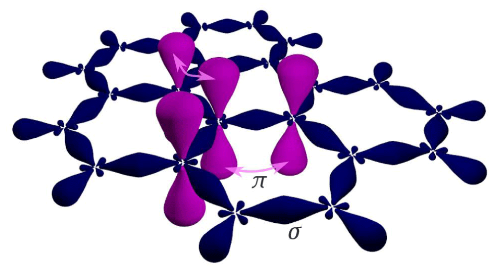
Figure 2: Schematic representation of σ- and π-bonding in graphene.
Efforts to induce magnetism in graphene have focused on breaking its structural symmetry to release unpaired electrons and generate net spin polarization. Magnetic ordering can arise when unpaired spins on adjacent carbon atoms or lattice sites interact strongly enough to align periodically, forming magnetic clusters or long-range magnetic order.
Over the past decade, two significant experimental breakthroughs have validated earlier theoretical predictions on magnetism in graphene:
- Point defects—such as vacancies, adatoms, or edge irregularities—can effectively induce localized magnetic moments by disrupting electron pairing.
- Bilayer graphene systems, where spins are localized on opposing faces of the two sheets, can couple ferromagnetically or antiferro magnetically, depending on stacking geometry and external conditions, leading to spin cluster formation.
Despite this progress, precise spatial control over spin distribution remains a formidable challenge, limiting current applications in spintronics and magnetic devices.
Recent advances in nanotechnology have significantly enhanced the exploration and application of graphene in various domains. As a two-dimensional (2D) carbon nanomaterial, graphene exhibits exceptional electrical, thermal, mechanical, and optical properties, making it a subject of intense academic interest and industrial relevance.
Graphene has enabled substantial progress in the development of:
- Electronic devices, including field-effect transistors and integrated circuits;
- Thermoelectric and optoelectronic systems;
- High-performance sensors and energy harvesting applications.
Mechanically, graphene displays:
- An exceptionally high Young’s modulus (~1 TPa);
- Intrinsic strength (~130 GPa);
- High stiffness and fracture strain; which makes it ideal for nanocomposite coatings, paints, flexible electronics, and biomedical applications [6].
The development of graphene-based nanocomposites remains a vibrant area of research due to the material’s unique structure and multifunctional behavior [7].
Additionally, graphene exhibits a range of novel quantum and transport phenomena, including:
- The anomalous quantum Hall Effect.
- The ambipolar electric field effect.
- The Klein tunneling effect.
- Ballistic transport over submicron scales.
These properties stem from graphene’s linear band dispersion near the Dirac points and its two-dimensional honeycomb crystal symmetry.
Moreover, the band gap of multilayer graphene-especially when studied through Raman spectroscopy and layer-stacking interactions significant commercial implications [8]. By engineering its nanostructure, including:
- Boundary configuration,
- Structural defects,
- Chemical doping,
- Formation of heterostructures,
Researchers can tune the electronic, optical, thermoelectric, and photothermal properties of graphene to meet the requirements of next-generation energy and electronic systems [9]. These modifications aim to achieve high energy density, low cost, and material stability, all essential for future transportation technologies and smart grid storage solutions.
Sigma (σ) bonds result from the overlap of sp² hybrid orbitals, forming strong in-plane bonds. Pi (π) bonds arise from the lateral overlap of pz orbitals, which extend perpendicularly to the graphene plane. For clarity, only one pz orbital and its three nearest neighbors are shown.
1.3 Dispersion and spin orders
In graphene, when atoms are positioned on its hexagonal lattice, the pz (π) orbitals-responsible for out-of-plane bonding-do not overlap with the px and py orbitals due to symmetry constraints. As a result, the pz electrons, which form the π bands, can be treated independently from the in-plane σ-electron system (Figure 2).
Within this π-band approximation, the tight-binding model, restricted to first-nearest-neighbor interactions, yields the electronic dispersion relation that defines the energy of electrons as a function of their wave vector in reciprocal space [10,11].
Remarkably, at low energies near the Dirac points, even without considering real spin, the electron dynamics in graphene can be described by a massless Dirac equation. Consequently, the low-energy quasiparticles in graphene behave as massless Dirac fermions, exhibiting linear energy–momentum dispersion. This pseudo-relativistic behavior is valid in the chiral limit, where the rest mass M0 approaches zero [10,12].
The ability to modulate the effective mass in graphene introduces novel functionalities. If mass gaps can be engineered-e.g., via substrate interactions, chemical doping, or bilayer twisting-electrons can be confined to massless regions surrounded by massive domains. This concept allows for the fabrication of quantum dots, quantum wires, and other mesoscopic structures within a single graphene sheet.
Moreover, such boundary-defined structures can give rise to one-dimensional conducting channels that are topologically protected against backscattering. These dissipationless edge modes hold great promise for future applications in quantum electronics, low-power interconnects, and spintronic devices [13].
1.4 Electron transport and spintronics orders
Graphene exhibits exceptional electron mobility at room temperature, with measured values exceeding 15,000 cm²· V¹ · s¹. Due to its symmetric band structure, hole and electron mobilities are expected to be nearly identical [14]. Interestingly, the mobility remains nearly temperature-independent between 10 K and 100 K, suggesting that defect scattering is the dominant limiting mechanism in this range [15].
At room temperature, the intrinsic limit to mobility set by acoustic phonon scattering is estimated to be as high as 200,000 cm²· V¹ · s¹ for a carrier density of 10^{12} cm}^{-2} [16,17]. This value is an order of magnitude greater than copper [18]. The corresponding resistivity of ideal graphene sheets is on the order of 10^ {-6} Ω · cm, which is lower than that of silver, the most conductive elemental metal.
However, charge transport in practical graphene devices is influenced by extrinsic factors, such as adsorption of contaminants (e.g., water and oxygen molecules) that can dope the surface and alter carrier density. Two dominant transport regimes are typically observed:
- A ballistic transport mode, which is temperature-independent and allows electrons to propagate over long distances without scattering.
- A thermally activated mode, characterized by increased resistance at shorter length scales and higher temperatures.
In the ballistic regime, electrons in graphene behave similarly to those in cylindrical carbon nanotubes. At room temperature, a significant resistance jump is observed at specific channel lengths: approximately 16 micrometers for ballistic transport, and around 160 nanometers for the thermally activated mode. Even at ambient conditions, electrons in graphene can traverse micrometer-scale distances without scattering, a property critical for nanoelectronic applications [19].
Graphene is widely regarded as a promising platform for spintronics due to it’s:
- Weak spin–orbit coupling,
- Low hyperfine interaction, owing to the negligible nuclear magnetic moment of carbon-12,
- Potential for long spin coherence times.
Experimental demonstrations have shown successful electrical spin injection and detection in graphene up to room temperature [20-22]. Additionally, spin coherence lengths exceeding 1 micrometer at room temperature have been observed, with electrical gate control of spin current polarity achieved at cryogenic temperatures [21].
In ultra-clean graphene, charged carriers behave like a strongly interacting, quasi-relativistic plasma, exhibiting hydrodynamic transport. In such regimes, electrons move collectively in a fluid-like manner, along preferred paths with frequent inter-particle collisions. This behavior has been observed in high-purity graphene encapsulated between hexagonal boron nitride (h-BN) layers, which suppresses extrinsic disorder and phonon scattering [23].
Graphene can also exhibit simultaneous magnetic and spintronic properties [24]. For instance, low-defect graphene nanomeshes, synthesized using non-lithographic fabrication techniques, demonstrate robust ferromagnetic behavior even at room temperature. In such nanostructures:
- A spin pumping effect is observed under in-plane magnetic fields,
- A magnetoresistance hysteresis loop emerges when magnetic fields are applied perpendicularly.
These phenomena open new possibilities for magneto-spintronic devices, where both charge and spin degrees of freedom are harnessed within a single material framework.
Graphene, a single atomic layer of carbon atoms arranged in a two-dimensional honeycomb lattice, exhibits a unique and anomalous form of the Quantum Hall effect (QHE). Unlike conventional two-dimensional electron systems, where the Hall conductivity is quantized in integer multiples of e^2/h, graphene demonstrates half-integer quantization, with an additional factor of 4 due to spin and valley degeneracy. Specifically, the Hall conductivity in graphene follows the sequence: σ {xy} = 2 e^2/h (e is the elementary charge and h is Planck’s constant).
This anomalous quantization arises from the relativistic-like behavior of graphene’s low-energy charge carriers, which behave as massless Dirac fermions. In the presence of a perpendicular magnetic field, these carriers occupy Landau levels, one of which forms precisely at zero energy, corresponding to the Dirac point.
The quantum Hall effect itself is a quantum mechanical manifestation of the classical Hall effect, wherein an applied magnetic field induces a transverse voltage perpendicular to an electric current. In its quantum version, observed at low temperatures and high magnetic fields, the transverse conductivity becomes quantized in discrete steps, reflecting the underlying topological nature of the electronic states [25].
The half-integer shift in graphene’s Hall quantization can be understood in terms of topological and geometrical concepts. Specifically, the Atiyah–Singer index theorem, a foundational result in differential geometry, relates the analytical index of an elliptic differential operator on a manifold to its topological index. This theorem has been invoked to explain the presence of the +1/2 term in the Hall conductivity of charge-neutral graphene, where the zero-energy Landau level contributes asymmetrically due to the chiral symmetry of the Dirac spectrum [26,27].
2.1 Polarity of graphene components
Graphene nanoparticles with varying degrees of oxidation-from low-polarity few-layer graphene (FLG, 3-5 layers) to high-polarity Graphene Oxide (GO), were synthesized using a one-step, cost-effective electrochemical exfoliation technique. The influence of electrolyte composition on the surface polarity of the exfoliated particles was investigated under identical conditions of current, oxidizing agent concentration, and electrolyte molarities (0.2 M). The electrolytes used include (NH₄)₂SO₄ (neutral), sodium dodecyl sulfate (SDS, basic), and HNO₃ (acidic) [28].
The exfoliated graphene samples were obtained without post-processing and characterized using multiple techniques, including X-ray Diffraction (XRD), Fourier-transform Infrared Spectroscopy (FT-IR), Thermo Gravimetric Analysis (TGA), Raman spectroscopy, and UV–Vis spectroscopy.
The results revealed distinct differences in the C/O ratio and component composition depending on the electrolyte used:
- (NH₄)₂SO₄ (neutral electrolyte): yielded a mixture of few-layer graphene and unreacted graphite, with a C/O ratio of 4.21.
- SDS (basic electrolyte): produced a mixture of FLG, GO, and unreacted graphite, with a C/O ratio of 2.21.
- HNO₃ (acidic electrolyte): generated a product consisting of 96.2% GO and 3.8% unreached graphite, with a significantly lower C/O ratio of 1.22, lower than that of samples synthesized via the conventional Hummers’ method.
These findings indicate that surface polarity can be precisely tuned by altering the electrolyte composition, enabling the tailored synthesis of graphene nanoparticles for specific applications [28]. A visual comparison of low- and high-polarity graphene components is provided in Figure 3. Figure 3 is used to compare the pgpz sample synthesized in this study with the reference samples reported in [28]. As illustrated in Figure 4d, our sample-prepared using a strong acidic electrolyte method (Figure 4b), exhibits notable differences. The synthesis procedure follows the protocols detailed in [8,29].
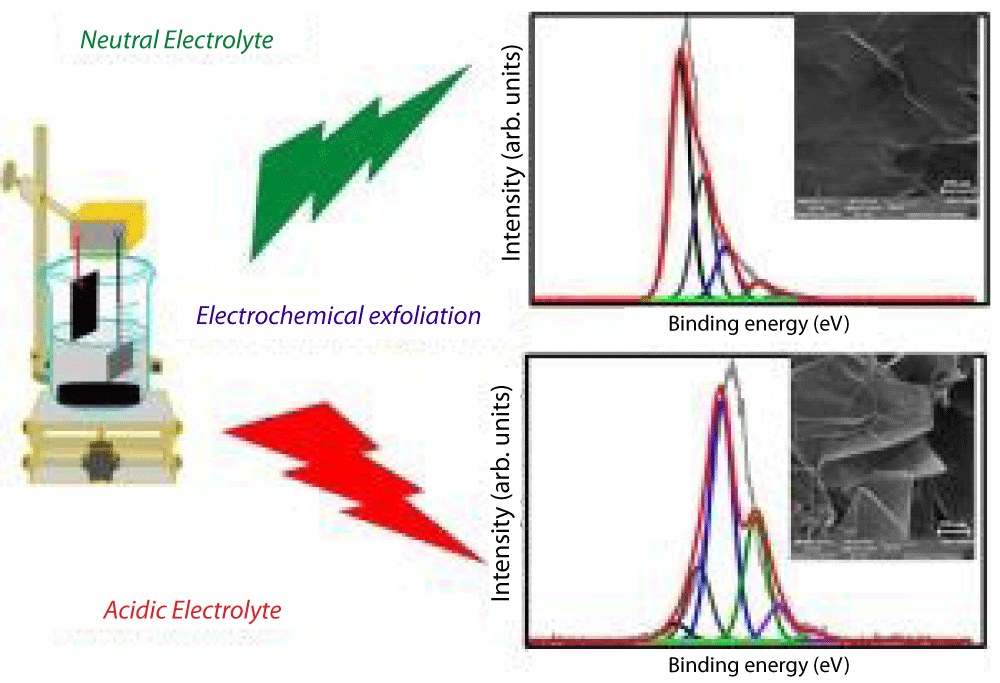
Figure 3: Schematic representation of low-polarity and high-polarity graphene components [28].
Further, using H₂SO₄ (strong acidic electrolyte) produced a high-polarity graphene sample, composed primarily of graphene oxide (GO, 11.54%) and partially reduced graphene oxide (PRGO, 22.21%), along with graphene nano-sheets (GNs, 66.25%). The resulting product is referred to as the pgpz sample. The dramatic change in surface polarity, attributed to electrolyte type, provides a means for controlled production of graphene particles with specific surface chemistry suitable for functional applications (XRD analysis with Cu Kα radiation) [8,29].
Table 1 presents the particle size distribution and compositional derivatives of the pgpz sample, as characterized in reference [29].
| 2. Graphene in spintronics: Particle size distribution and component percentages for the pgpz sample. | |||||||
| Components λ=0.15406nm |
2θ Angle |
d-spacing (nm) | FWHM (2θ) |
Shape Factor SF |
Average Particle. Size (nm) |
Sample Size% | |
| 1 | GO. | 11.543 | 0.766162 | 0.0900 | 1.00 | 98.08. | 11.54 |
| 2 | PRGO. | 19.449 | 0.456257 | 4.0000 | 0.94 | 2.10 | 22.21 |
| 3 | GNs. | 26.250 | 0.339225 | 3.4428 | 1.10 | 2.82 | 66.25 |
The UV–Vis absorption spectrum of the pgpz sample (Figure 4f) highlights three prominent peaks:
- 238 nm: associated with GO (π–π* transitions of aromatic C=C),
- 271 nm: indicative of graphene nanosheets,
- 298 nm: corresponding to PRGO, reflecting partial reduction of oxygen functional groups.
Using the Tauc plot method (Figure 4d), the estimated band gap energies corresponding to graphene at 271 nm and its derivatives are summarized in Table 2. The data in Figure 4d show significantly higher polarity compared to the reference sample in Figure 4a [28], primarily due to the use of a strong acidic electrolyte during synthesis. Supporting evidence from the XRD spectrum (Figure 4c) and FE-SEM image (Figure 4e) further corroborates these differences in the structural and morphological characteristics of our sample (Figure 4b).
| Table 2: Estimated Band Gap Energies of Graphene Components. | |
| Components | Band Gap Energy (eV) |
| Graphene Oxide (GO) | ~2.13 - 3.5 eV |
| Partially reduced graphene oxide (PRGO) | ~0.3 - 1.5 eV |
| Graphene (GNs) | ~2.12 eV |
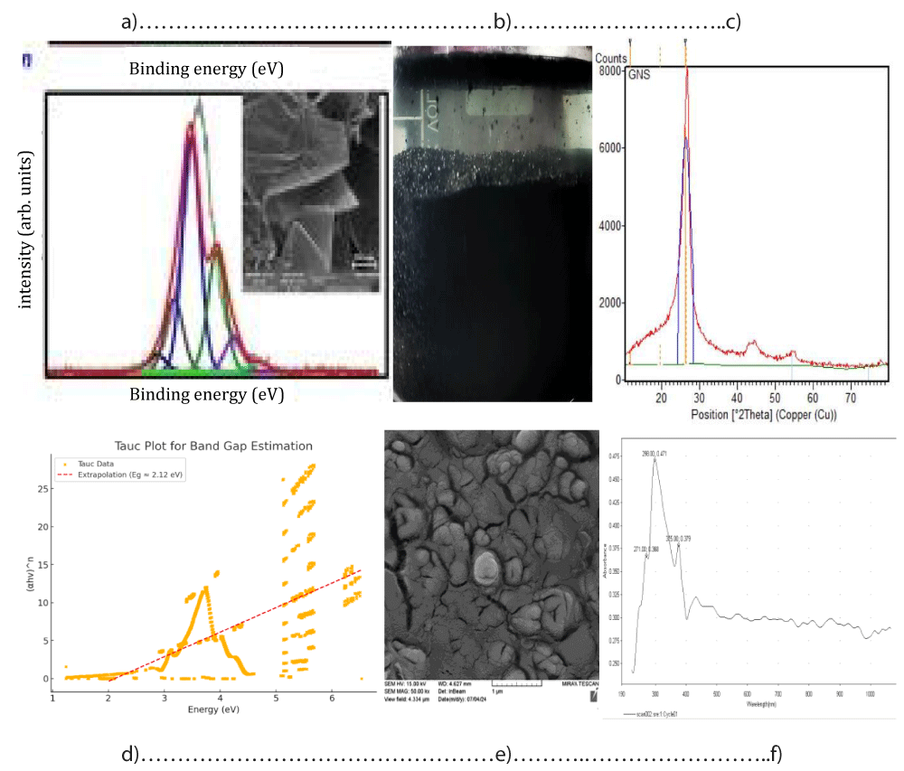
Figure 4: Top row, a-c (from left to right); high polarity sample [28], middle, the pgpz sample synthesized in strong acidic electrolyte, right XRD spectrum highlighting the graphene diffraction peak. Bottom row, d-f (from left to right); higher polarity binding energy, middle FE-SEM, and right UV–Vis spectrum of the pgpz sample [29].
As is well known, bilayer twisted graphene exhibits relatively high binding energy (BE), which refers to the energy required to disassemble an atom or molecular system into its constituent parts. While the typical band gap for multilayer graphene sheets lies between 1–2 eV, the values observed in our sample (Table 2) exceed this range, which can be attributed to the increased surface polarity as evidenced in Figure 4d.
Raman spectroscopy was also used for further analysis of the pgpz sample (Figure 5). The Raman intensity ratios are consistent with multilayer graphene:
ID/IG = 135/156 = 0.865 (indicating multilayer graphene)
I2D/IG = 44/156 = 0.282 (confirming multilayer graphene)
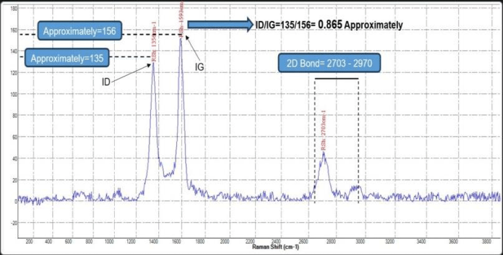
Figure 5: Raman shift spectrum of the pgpz sample, showing D, G, and 2D peaks [29].
2.2 Application of TEM and AFM images of the pgpz sample
Transmission Electron Microscopy (TEM) uses a focused beam of electrons to image a sample by transmitting the normal beam through it. Recent work has used TEM to investigate the temperature dependence of the structure of graphene oxide, focusing in particular on the placement of the oxygen atoms around the carbon lattice. Because of the small de Broglie wavelength of electrons, TEM offers resolution thousands of times higher than the resolution of light microscopes. Thus, since its invention in 1931, TEM has become a prime analytical method in the physical, chemical, and biological sciences. Graphene-covered TEM grids are especially proving to be useful for biotechnology, because biological samples tend to stick to the walls of the holes in uncovered TEM grids, distorting shape and adversely affecting resolution. Graphene solves that problem and is even compatible with cryogenic TEM, because it can sustain large temperature variations.
In the case of graphene, a particular morphology is chosen to tune the material properties for the desired applications [30]. However, it is not always obvious or easy to identify by simple visual inspection or testing of the sample whether the graphene morphology is the correct one or not. What makes graphene a ‘wonder material’ is that the atomic structure means that it has many electrical properties that differentiate it from typical bulk carbon samples, including exceptionally high electron mobility? This can combine with the ability to create thin, flexible graphene sheets and the very high thermal conductivity of graphene, making it an excellent candidate for next-generation transistors [31]. In Figure 6, TEM images of the pgpz sample are shown at different magnification scales. Finally, the FFT filter is used to reveal the superimposed multilayer graphene topology shown in Figure 7.
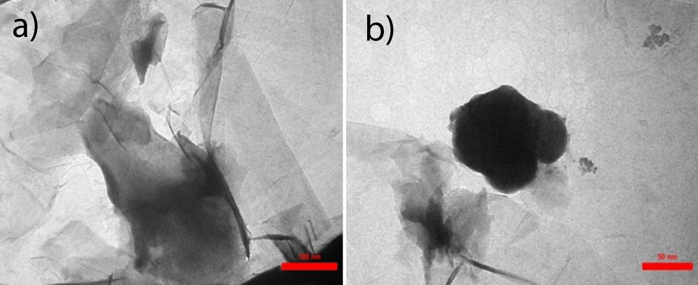
Figure 6: TEM images of the pgpz sample: (a) Low magnification of the graphene components. Featureless regions are atomically clean areas, while slightly darker grey patches are amorphous GO and PRGO contaminations. (b) High-resolution TEM image of amorphous contaminations (darker grey, GO and patches grey PRGO).
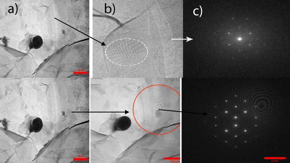
Figure 7: Detecting two areas of potential Moiré patterns on TEM images; (a) multilayer twisted graphene shown by arrow in (b), after removing the graphene multi-lattice by a fast Fourier filter (c). This can prove that the sample has multi-layer graphene sheets shown in Figure 5.
As discussed in Section 2.1, the pgpz sample comprises three primary graphene-derived components, each associated with a distinct band gap energy (see Table 2 and Figures 4d–4f). Raman spectroscopy analysis (Figure 5) revealed intensity ratios consistent with a multilayer graphene structure. These findings align with the Fast Fourier Transform (FFT) analysis shown in Figure 7c, which suggests the presence of Moiré patterns characteristic of twisted multilayer graphene.
Atomic force microscopy (AFM) or scanning force microscopy is a very-high-resolution type of scanning probe microscopy, with demonstrated resolution on the order of fractions of a nanometer or less, more than 1000 times better than the optical diffraction limit [32].
Atomic Force Microscopy (AFM) is well established as an analytic tool to image various properties of 2D and 3D nanomaterials, from simple topography to complex properties like moiré patterns emerging on twisted bilayers of graphene or hBN/graphene heterostructures. However, AFM also allows for controlled manipulation and fabrication of nanostructures and novel applications like mechanically reconfigurable devices.
AFM is now the instrument of choice for studying graphene components for two main reasons: resolution and availability of several different modes facilitating detailed characterization of graphene, including its mechanical and electrical properties beyond the topography. Achieving excellent 2D and 3D resolution is crucial when evaluating phenomena close to the atomic scale. Another application of AFM offers the available measurement modes to evaluate electrical and mechanical properties simultaneously with the topography. These modes can be applied to study additional properties in the quality of grown graphene or the angular mismatch between stacked graphene layers. Examples of its applications are 1) Topography, 2) Particle thickness, 3) Growth analysis, 4) Lattice mismatch, 5) Cutting graphene edges, etc. Figure 8 shows many different AFM Images from the pgpz samples in 2D. All necessary image processing and filtration techniques are applied to clean up the images. Topography, particle size distribution, and growth analysis are investigated for all images. The results are shown in Table 3.
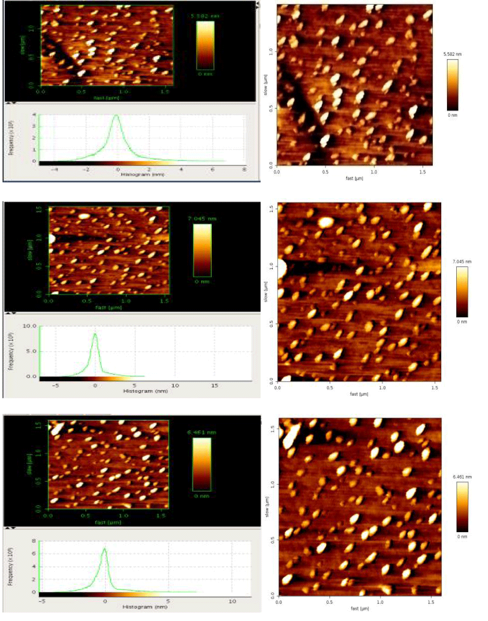
Figure 8: 2D non-contact AFM images are shown; Top, the maximum particle size distribution in color coded up to 5.584 nm. Middle, the maximum particle size distribution in color coded up to 7.654 nm, and bottom, the maximum particle size distribution in color coded up to 6.461 nm.
| : Roughness and size distribution of the pgpz sample shown in Figure 8. | |||||||
| Images | Physical image Size(nm2) |
Peak-to-Valley Roughness (nm) |
RMS Roughness (nm) |
Average Roughness (pm) |
Average Value (pm) |
Average Particle. Size (nm) |
Sample Size% |
| Top image | 1.59x1.41 | 13.06 | 1.269 | 832.4 | 1.256 | GO.98.08 | 11.54 |
| Middle image |
1.55x1.55 | 26.62 | 1.601 | 897.8 | 11.59 | PRGO.2.10 | 22.21 |
| Bottom image | 1.59x1.59 | 16.69 | 1.468 | 868.7 | 2.645 | GNs.2.82 | 66.25 |
In Figure 9, 3D-AFM images of the pgpz samples are shown. The maximum height of particles may reach up to 12 nm. Cutting edges of the multilayer graphene in panel 3 are also indicated by Raman spectroscopy in Figure 5.
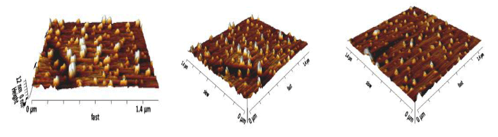
Figure 9: 3D-AFM images of the pgpz sample with 45-degree rotation.
2.3 Chirality of twisted graphene sheets
Chirality-the property of an object being non-superimposable on its mirror image-has become a pivotal concept in numerous scientific domains, including chiroptical sensing, biosensing, catalysis, and spintronics. In recent years, twisted two-dimensional (2D) materials have emerged as a novel class of atomically thin chiral structures, where chirality arises from the interlayer twist angle between stacked layers. These systems offer tunable chiral properties through precise control of twist geometry, enabling the design of materials with engineered electronic and optical responses.
Graphene, a prototypical 2D material, has played a central role in this development. Its twisted bilayer configurations-especially at the so-called magic angles-exhibit chiral behavior that is deeply intertwined with electronic phenomena such as flat bands, superconductivity, and strong correlation effects. The concept of chirality in bilayer graphene is illustrated in Figure 10, which aligns with the magic angle Dirac points previously discussed in [29,33].
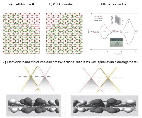
Figure 10: Chiral states in twisted bilayer graphene. (a) and (b): Schematic representations of left-handed and right-handed chiral stacking configurations. (c)Measured ellipticity spectra (Ψ) from left-handed (red), right-handed (blue) twisted bilayer graphene, and single-layer graphene (gray). Each chiral spectrum shows two distinct peaks, labeled as peak A and peak B, indicating strong chiroptical activity. (d): Top panels-electronic band structures of the left- and right-handed twisted bilayer graphene; Bottom panels-cross-sectional diagrams depicting the spiral atomic arrangements that give rise to structural chirality.
In Figure 11, the chirality introduced at the twisted interface of bilayer graphene is shown to propagate through additional stacked layers, resulting in a few-layer more chiral graphene with an enhanced chiroptical response. This phenomenon is confirmed via polarization-resolved Raman spectroscopy, which is highly sensitive to both chirality and symmetry breaking in the lattice.
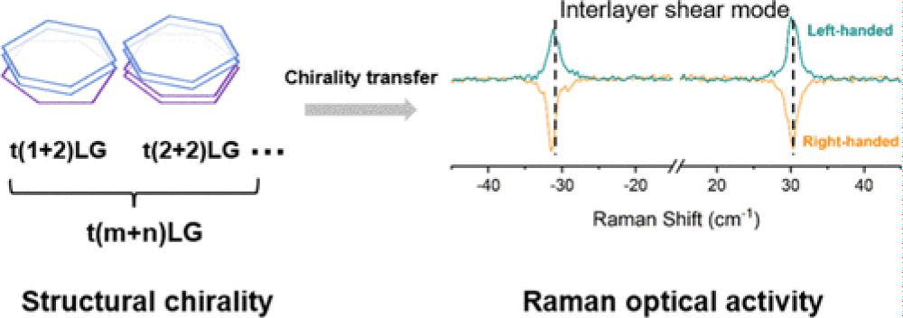
Figure 11: Structural chirality revealed via Raman optical activity.
This observation directly connects to the previously discussed pgpz sample, where increased polarity and multilayer chirality were identified using Raman spectral features (refer to Figure 5). The Raman Optical Activity (ROA) associated with structural chirality underscores the role of interlayer twist in modulating spin, optical, and quantum behaviors of twisted graphene systems.
Chiral Raman signatures observed in multilayer graphene samples, consistent with those reported in Figure 5 for the pgpz sample. Finally, the observed high polarity (Figures 10,11), along with the Moiré patterns and chirality evident in multilayer graphene (Figure 7c), provide strong evidence supporting electron spin polarization and the presence of Dirac points, as discussed in Conclusions #8 and #14.
Based on extensive spectral analysis, imaging data, and structural characterization, the pgpz sample demonstrates multiple important physical orders and material features. The key findings are summarized as follows:
This study demonstrates that the pgpz graphene sample, prepared via electrochemical exfoliation, possesses a combination of topological, topographical, electronic, and chiral orders. Comprehensive characterization using XRD, UV-Vis, Raman spectroscopy, FE-SEM, TEM, and AFM techniques confirms that such structures exhibit unique electronic properties, mechanical robustness, and enhanced surface polarity and chirality.
These findings position pgpz graphene as a promising candidate for advanced applications in quantum computing, superconductivity, spintronics, energy storage, and radiation shielding.
The authors gratefully acknowledge the financial support provided by PGPZ International for conducting this research.
- Kim S, Schwenk J, Walkup D, Zeng Y, Ghahari F, Le ST, et al. Edge channels of broken-symmetry quantum Hall states in graphene visualized by atomic force microscopy. Nature Communications. 2021;12(1):2852. Available from: https://doi.org/10.1038/s41467-021-22886-7
- Young AF, Sanchez-Yamagishi JD, Hunt B, Choi SH, Watanabe K, Taniguchi T, et al. Tunable symmetry breaking and helical edge transport in a graphene quantum spin Hall state. Nature. 2014;505(7484):528–32. Available from: https://doi.org/10.1038/nature12800
- Yao W, Yang SA, Niu Q. Edge states in graphene: From gapped flat-band to gapless chiral modes. Physical Review Letters. 2009;102(9):096801. Available from: https://doi.org/10.1103/PhysRevLett.102.096801
- Plotnik Y, Rechtsman MC, Song D, Heinrich M, Zeuner JM, Nolte S, et al. Observation of unconventional edge states in “photonic graphene”. Nature Materials. 2014;13(1):57–62. Available from: https://doi.org/10.1038/nmat3783
- Xu B-C, Xie B-Y, Xu L-H, Deng M, Chen W, Wei H, et al. Topological Landau–Zener nanophotonic circuits. Advanced Photonics. 2023;5(3):036005. Available from: https://doi.org/10.1117/1.AP.5.3.036005
- Wang H, Cao Q, Peng Q, Liu S. Atomistic study of mechanical behaviors of carbon honeycombs. Nanomaterials. 2019;9(1):109. Available from: https://doi.org/10.3390/nano9010109
- Sang M, Shin J, Kim K, Yu KJ. Electronic and thermal properties of graphene and recent advances in graphene-based electronics applications. Nanomaterials. 2019;9(3):374. Available from: https://doi.org/10.3390/nano9030374
- Sepehri A, Ghassem-Alaskari MK. The Feasibility of Synthesized Micro Graphene Particles. 9th International Conference on Research in Science and Engineering, KBU, Bangkok, Thailand, EN-P-543. 2025.
- Wang J, Mu X, Sun M. The thermal, electrical, and thermoelectric properties of graphene nanomaterials. Nanomaterials. 2019;9(2):218. Available from: https://doi.org/10.3390/nano9020218
- Semenoff GW. Condensed-matter simulation of a three-dimensional anomaly. Physical Review Letters. 1984;53(26):2449–52. Available from: https://doi.org/10.1103/PhysRevLett.53.2449
- Wallace PR. The band theory of graphite. Physical Review. 1947;71(9):622–34. Available from: https://doi.org/10.1103/PhysRev.71.622
- Lamas CA, Cabra DC, Grandi N. Generalized Pomeranchuk instabilities in graphene. Physical Review B. 2009;80(7):075108. Available from: https://doi.org/10.1103/PhysRevB.80.075108
- Fuhrer MS. Critical mass in graphene. Science. 2013;340(6139):1413–4. Available from: https://doi.org/10.1126/science.1240317
- Charlier J-C, Eklund PC, Zhu J, Ferrari AC. Electron and phonon properties of graphene: Their relationship with carbon nanotubes. In: Jorio A, Dresselhaus G, Dresselhaus MS, editors. Carbon Nanotubes: Advanced Topics in the Synthesis, Structure, Properties and Applications. Springer-Verlag; 2008.
- Morozov SV, Novoselov K, Katsnelson M, Schedin F, Elias D, Jaszczak J, Geim A. Giant intrinsic carrier mobilities in graphene and its bilayer. Physical Review Letters. 2008;100(1):016602. Available from: https://doi.org/10.1103/PhysRevLett.100.016602
- Chen JH, Jang C, Xiao S, Ishigami M, Fuhrer MS. Intrinsic and extrinsic performance limits of graphene devices on SiO₂. Nature Nanotechnology. 2008;3(4):206–9. Available from: https://doi.org/10.1038/nnano.2008.58
- Kusmartsev FV, Wu WM, Pierpoint MP, Yung KC. Application of graphene within optoelectronic devices and transistors. arXiv preprint, arXiv:1406.0809. 2014. Available from: https://arxiv.org/abs/1406.0809
- Neto AHC, Peres NMR, Novoselov KS, Geim AK. The electronic properties of graphene. Reviews of Modern Physics. 2009;81(1):109–62. Available from: https://doi.org/10.1103/RevModPhys.81.109
- Novoselov KS, Geim AK, Morozov SV, Jiang D, Katsnelson MI, Grigorieva IV, et al. Two-dimensional gas of massless Dirac fermions in graphene. Nature. 2005;438(7065):197–200. Available from: https://doi.org/10.1038/nature04233
- Tombros N, Jozsa C, Popinciuc M, Jonkman HT, van Wees BJ. Electronic spin transport and spin precession in single graphene layers at room temperature. Nature. 2007;448(7153):571–4. Available from: https://doi.org/10.1038/nature06037
- Cho S, Chen Y-F, Fuhrer MS. Gate-tunable graphene spin valve. Applied Physics Letters. 2007;91(12):123105. Available from: https://doi.org/10.1063/1.2784934
- Ohishi M, Shiraishi M, Nakanishi T, Suzuki Y. Spin injection into a graphene thin film at room temperature. Japanese Journal of Applied Physics. 2007;46(25):L605–7. Available from: https://doi.org/10.1143/JJAP.46.L605
- Borghino D. Liquid-like graphene could be the key to understanding black holes. New Atlas. 2016 Feb 15. Available from: https://newatlas.com/liquid-graphene-dirac-fluid/41801/
- Hashimoto T, Kamikawa S, Yagi Y, Haruyama J, Yang H, Chshiev M. Graphene edge spins: Spintronics and magnetism in graphene nanomeshes. Nanosystems: Physics, Chemistry, Mathematics. 2014;5(1):25–38. Available from: https://nanojournal.ifmo.ru/en/wp-content/uploads/2014/02/NPCM51_P25-38.pdf
- Bolotin KI, Ghahari F, Shulman MD, Stormer HL, Kim P. Observation of the fractional quantum Hall effect in graphene. Nature. 2009;462(7270):196–9. Available from: https://doi.org/10.1038/nature08582
- Gusynin VP, Sharapov SG. Unconventional integer quantum Hall effect in graphene. Physical Review Letters. 2005;95(14):146801. Available from: https://doi.org/10.1103/PhysRevLett.95.146801
- Zhang Y, Tan Y-W, Stormer HL, Kim P. Experimental observation of the quantum Hall effect and Berry’s phase in graphene. Nature. 2005;438(7065):201–4. Available from: https://doi.org/10.1038/nature04235
- Kim M, Hwang HM, Park GH, Lee H. Graphene-based composite electrodes for electrochemical energy storage devices: Recent progress and challenges. FlatChem. 2017;6:48–76. Available from: https://doi.org/10.1016/j.flatc.2017.08.002
- Ghassem-Alaskari MK, Sepehri A, Kassaee MZ. Unlocking Graphene’s Potential: Size Distribution and Topological Advances. International Journal of Physics Research and Application. 2025. Available from: https://doi.org/10.1016/j.jics.2024.101173
- Le Ferrand H, Chabi S, Agarwala S. 3D assembly of graphene nanomaterials for advanced electronics. Advanced Intelligent Systems. 2020;2(5):1900151. Available from: https://doi.org/10.1002/aisy.201900151
- Yan Z, Nika DL, Balandin AA. Thermal properties of graphene and few-layer graphene: Applications in electronics. IET Circuits, Devices & Systems. 2015;9(1):4–12. Available from: https://doi.org/10.1049/iet-cds.2014.0093
- Binnig G, Quate CF, Gerber C. Atomic force microscope. Physical Review Letters. 1986;56(9):930–3. Available from: https://doi.org/10.1103/PhysRevLett.56.930
- Kim CJ, Sánchez-Castillo A, Ziegler Z, Ogawa Y, Noguez C, Park J. Chiral atomically thin films. Nat Nanotechnol. 2016;11(6):520–4. Available from: https://doi.org/10.1038/nnano.2016.3